Mechanical design is one of the main reasons teams move from a standard board to a custom SBC. A standard development board may work electrically, but it may not fit the enclosure, align with connector openings, route display cables cleanly, leave space for antennas, or support fast assembly. These problems become expensive when they are discovered after the industrial design is frozen.
For Custom SBC Mechanical Design: PCBA Outline, Mounting Holes, Connectors, and Enclosure Fit, the most useful factory question is whether the test can catch the failure before shipment. Power, flashing, display, touch, wireless, Ethernet, serial ports, audio, storage, buttons, and product-specific functions need a practical pass/fail path with traceable results.
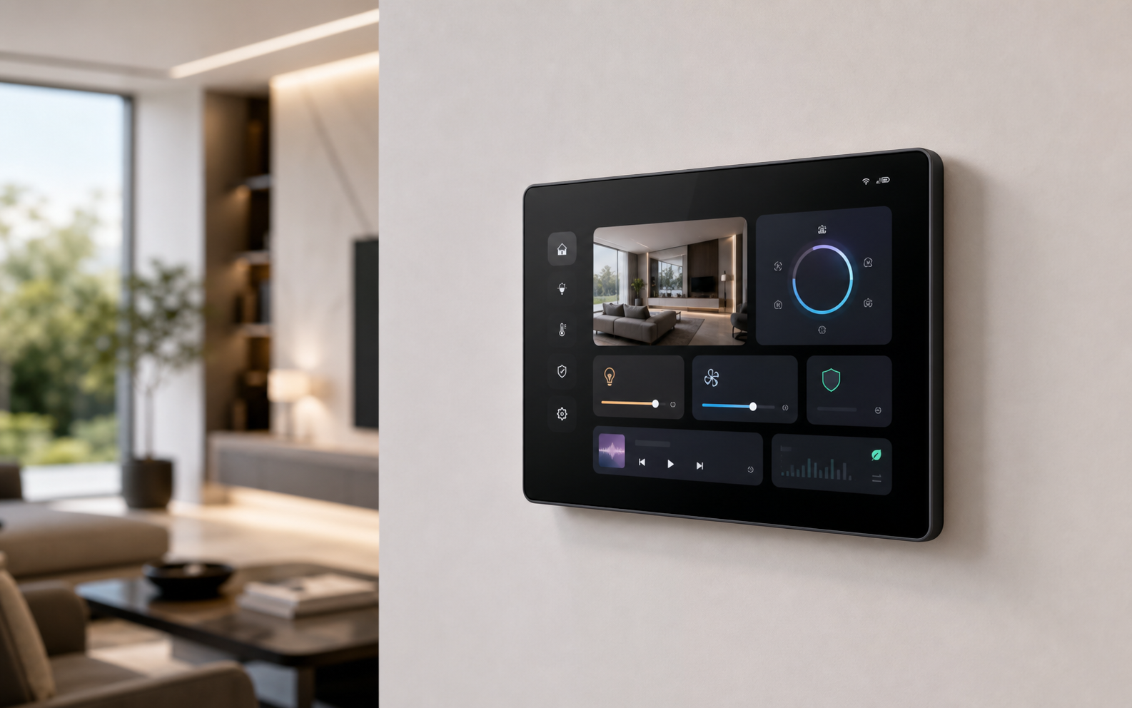
A Custom SBC should be designed around the final product enclosure, not only around the schematic. PCBA outline, mounting holes, connector placement, component height, thermal position, antenna clearance, and service access all affect whether the board can become a product.
Start with product drawings
Before layout begins, prepare enclosure drawings, screen position, connector openings, mounting bosses, cable paths, speaker and microphone positions, camera window, battery space, antenna zone, and maximum component height. If the product already has a mold or industrial design, the board must respect those constraints. If the enclosure is still flexible, board and enclosure design need review together.
For Android display products, compare Android SBC requirements around display, touch, speaker, microphone, camera, and wireless. For gateway and control products, compare Linux SBC and Industrial SBC requirements around field wiring, terminal access, and service ports.
Key mechanical items
| Mechanical item | Why it matters |
|---|---|
| PCBA outline | Determines enclosure fit and available routing space |
| Mounting holes | Affects assembly strength and vibration behavior |
| Connector direction | Affects cable routing, port openings, and service access |
| Component height | Affects enclosure depth and thermal clearance |
| Display cable path | Affects EMI, bend radius, assembly time, and reliability |
| Antenna position | Affects Wi-Fi, Bluetooth, LTE, and product performance |
| Test points | Affects factory fixture design and production speed |
These items need review before PCB layout is locked. Moving a connector after layout can affect routing, signal integrity, enclosure tooling, and test fixture design.
Connector placement is a product decision
Connectors are not only electrical components. They define how installers, users, factory technicians, and service teams interact with the product. External connectors must match openings. Internal connectors must be reachable during assembly. Factory-only connectors should be accessible without damaging the enclosure.
For gateways and controllers, terminal blocks may need a clear wiring direction and enough spacing for field installation. For HMI and smart terminals, display, touch, camera, speaker, microphone, and antenna cables need predictable routes. A custom board can reduce adapter cables and make the product easier to build.
Connector decisions should also consider lifecycle and purchasing. A connector that looks convenient in the prototype may be difficult to source later, may need manual soldering, or may not survive repeated service use. Procurement needs to confirm availability and acceptable alternates, while engineers confirm current rating, mating direction, retention force, and cable assembly method.
Display, touch, and antenna constraints
Display products often have strict mechanical requirements. LCD cable length, touch FPC direction, backlight wiring, speaker cavity, microphone opening, and front cover structure can all influence board shape. Antenna placement should avoid metal shielding, noisy power areas, and enclosed corners when possible.
The official KiCad documentation is useful background for PCB design workflows, but production mechanical fit depends on the actual enclosure, selected connectors, cables, and assembly method.
Thermal and service planning
Thermal issues often appear after the PCB is placed inside the enclosure. The processor, PMIC, wireless module, power input, and display backlight can all create heat. The design should consider airflow, heat spreading, component location, and whether the product operates in a sealed housing.
Service access should also be planned. Debug UART, USB service port, reset button, recovery mode, and test pads may be needed during development and production. If these are hidden after assembly, failure analysis becomes slower.
Production assembly review
Mechanical design should be checked from the factory’s point of view. Can workers insert cables without special tools? Are connectors keyed? Can the fixture contact test points? Can labels be applied? Can the board be removed if needed? Can the antenna be installed consistently?
For a broader custom board path, read Custom SBC Design from Enclosure to Production and Custom SBC Development Process: From Requirements to EVT, DVT, PVT, and Production.
During pilot production, ask the assembly team to record slow or error-prone steps. If workers need to bend a cable sharply, hold a connector at an awkward angle, or remove the board to access a test point, the design may need another review. These issues are small in a ten-piece sample build but costly across hundreds or thousands of units.
Final recommendation
Plan custom SBC mechanical design as early as schematic architecture. The board outline, connectors, mounting holes, display route, antenna zone, thermal layout, and test access should support the final product, not fight it. That is where custom board development creates real production value.
Frequently Asked Questions
What details are useful before we talk about a Custom SBC build?
Send the use case, OS preference, display or I/O list, enclosure limits, power input, wireless needs, target quantity, and timing. With that context, Avontek can suggest a Custom SBC hardware path that fits the real device instead of only comparing board specifications.
When is a custom SBC worth considering for a Custom SBC product?
A custom SBC is worth reviewing when the device needs a fixed PCBA outline, connector position, display interface, power input, wireless module, mounting method, or cost target that a catalog board cannot meet cleanly.
Can Avontek stay involved after Custom SBC samples are built?
Yes. Avontek can help with Custom SBC board choice, Android or Linux BSP discussion, peripheral checks, sample bring-up, test fixtures, image review, and factory coordination.