A custom SBC project should not start with PCB layout. It should start with a clear product requirement: what the device does, where it will be installed, which operating system it runs, what interfaces it exposes, how it fits the enclosure, and how it will be tested in production. Without that structure, the board may work as a prototype but fail as a repeatable product.
For Custom SBC Development Process: From Requirements to EVT, DVT, PVT, and Production, separate cosmetic preferences from engineering blockers before the layout starts. Connector clashes, antenna position, heat sources, power input, and fixture access usually deserve early design time; small preferences can often wait until the next revision if they do not affect production or safety.
For embedded products, a Custom SBC is usually considered when a standard board does not match the enclosure, connector layout, display interface, power input, I/O list, wireless module, cost target, or production process. The development path should connect hardware, BSP, mechanical design, application testing, and manufacturing from the beginning.
Requirement definition
The first step is to collect product information. Engineers should define processor direction, operating system, display and touch, Ethernet, USB, UART, RS485, CAN, GPIO, camera, audio, wireless, power input, storage, buttons, LEDs, and service ports. Project managers should define schedule, sample quantity, pilot run target, certification needs, and launch timing. Procurement should define expected volume, cost target, lifecycle needs, and preferred component restrictions.
If the processor family is not fixed, compare Rockchip SBC and Allwinner SBC directions before schematic work begins. If the OS is already fixed, review Android SBC or Linux SBC requirements so the BSP scope is realistic.
| Phase | Main output | Main risk if skipped |
|---|---|---|
| Requirements | Interface list, OS, enclosure, quantity, test goals | Board solves the wrong problem |
| Architecture | SoC, memory, storage, power, peripherals | Performance or interface mismatch |
| Schematic | Circuit design and component selection | Rework after prototype bring-up |
| PCB layout | Board outline, routing, placement, DFM checks | Mechanical or signal integrity issues |
| EVT | First engineering validation | Hidden hardware and BSP problems |
| DVT | Design validation under product conditions | Field behavior not verified |
| PVT | Pilot production validation | Factory process not repeatable |
Architecture and schematic design
Architecture decisions include SoC, PMIC, memory, storage, Ethernet PHY, wireless module, audio codec, display interface, touch controller, power protection, and expansion interfaces. These choices affect cost, driver support, supply, thermal behavior, and layout complexity.
Schematic review needs to cover the board supplier, customer engineering team, and sometimes the display or module supplier. A small component decision can affect Android BSP, Linux device tree, factory testing, and purchasing. This is why component selection should not be treated as a purely electrical task.
At this stage, the team should also separate fixed requirements from negotiable requirements. Fixed items may include enclosure size, display model, field connector position, operating system, or required communication protocol. Negotiable items may include memory size, storage capacity, wireless module model, connector series, or exact SoC within the same platform family. This distinction helps the supplier propose practical changes without weakening the product goal.
For project managers, the main checkpoint is whether the design can still meet schedule and production quantity. For procurement, the checkpoint is whether long-lead components and risky ICs are visible before prototypes are ordered.
What the customer should prepare before design starts
A custom SBC project moves faster when the customer provides real product context, not only a list of interfaces. Useful inputs include enclosure drawings, target display datasheets, touch panel information, cable direction, wall or machine mounting details, power supply conditions, expected operating temperature, software workflow, application startup behavior, communication protocol list, certification expectations, target quantity, and launch schedule.
Photos or samples of the previous product are also valuable. They show connector positions, service access, common installation habits, and what the new board must improve. If the product is part of a system, explain what connects to it and what happens when network, power, or peripheral devices fail. These details help the hardware team design for actual use instead of ideal lab conditions.
It is equally important to define who owns each deliverable. Some customers expect the supplier to provide a complete Android or Linux image, production flashing tool, factory test program, and sample debugging support. Others only need hardware design and BSP baseline. Both models can work, but the responsibility split should be clear before schematic work begins.
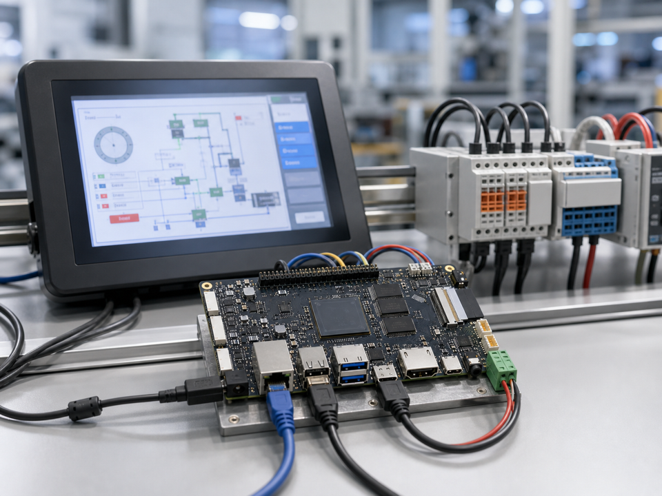
PCB layout and mechanical fit
PCB layout must match the final product. Board outline, mounting holes, connector direction, cable bend radius, component height, antenna location, test points, thermal areas, and service access all matter. A board that is electrically correct can still be difficult to assemble if connectors face the wrong direction or test points are unreachable.
The official IPC standards resources are useful background for electronics manufacturing expectations, but each custom SBC still needs project-specific DFM and test planning.
At layout review, do not only look at whether the board fits the outline. Check how the operator will plug in cables, where the antenna sits, whether heat is trapped under the display, whether test pins are accessible, and whether screws or plastic posts conflict with tall components. These details are ordinary, but they often decide whether factory assembly feels clean or awkward.
For boards with displays, camera, high-speed USB, Ethernet, wireless, or long external cables, ask for an explicit review of signal routing and grounding. For industrial products, also review protection around external interfaces. A custom board is an opportunity to remove adapters and weak wiring from the product, so the layout should make the final unit easier to build and test.
EVT, DVT, and PVT
EVT validates the first engineering samples. It should check power rails, boot behavior, interfaces, display, touch, wireless, storage, thermal condition, and basic BSP. DVT validates the design under product conditions, including enclosure, cable routing, application workflow, power recovery, and longer operation. PVT validates the pilot production process: assembly, flashing, fixture testing, labels, packaging, and issue feedback.
The most useful EVT reports are specific. Instead of only saying “USB OK” or “display OK,” record the tested port, device, image version, cable, test duration, and any limitation. DVT should move closer to real use: board in enclosure, real power supply, real display, real application, expected room or cabinet temperature, and the same cable lengths planned for production. PVT should prove that the factory can build more than a few good samples with a repeatable process.
Custom SBC validation flow:
1. Bring up power, bootloader, and system image.
2. Verify every interface against the requirement list.
3. Test the board inside the product enclosure.
4. Run application and BSP stability checks.
5. Build pilot units with factory flashing and test fixtures.
6. Release only after failures are tracked and closed.
BSP and production release
Custom board release needs to cover a stable Android or Linux image, flashing method, version naming, supported peripheral list, known limitations, and factory test procedure. Read Android and Linux BSP Driver Support for SBC Projects for broader BSP context and PCBA Production Testing for Embedded SBC Projects for production checks.
The final production decision should be based on verified hardware, verified software, verified enclosure fit, and verified factory process. A prototype that boots once is not a production-ready custom SBC.
Before release, prepare a simple acceptance checklist that both customer and supplier can sign off. It needs to cover tested hardware functions, system image version, application version, known open issues, approved BOM, test fixture status, packaging requirement, and pilot run result. This reduces confusion when the first production order is placed.
What not to customize too early
Not every difference deserves a custom design on day one. If the product is still exploring market demand, a standard SBC with a simple adapter or development cable may be enough for application testing. Customization makes sense when the requirement is stable: enclosure, screen, ports, power, wireless, cost target, and expected volume are known. Starting too early can create rework when the product manager changes the screen size or the customer asks for a different installation method.
The safer approach is to use standard boards for software proof, then freeze the product requirements before the custom schematic. Once EVT begins, changes should be controlled. A late connector change may also change PCB layout, enclosure tooling, cable design, test fixture, and documentation. Treat hardware changes after EVT as project decisions, not casual improvements.
For purchasing, the best time to discuss cost reduction is after the product architecture is stable but before DVT is closed. At that stage, the supplier can review component alternatives, assembly simplification, test fixture design, and packaging without breaking the basic product direction.
Frequently Asked Questions
What details are useful before we talk about a Custom SBC build?
Send the use case, OS preference, display or I/O list, enclosure limits, power input, wireless needs, target quantity, and timing. With that context, Avontek can suggest a Custom SBC hardware path that fits the real device instead of only comparing board specifications.
When is a custom SBC worth considering for a Custom SBC product?
A custom SBC is worth reviewing when the device needs a fixed PCBA outline, connector position, display interface, power input, wireless module, mounting method, or cost target that a catalog board cannot meet cleanly.
Can Avontek stay involved after Custom SBC samples are built?
Yes. Avontek can help with Custom SBC board choice, Android or Linux BSP discussion, peripheral checks, sample bring-up, test fixtures, image review, and factory coordination.