A custom SBC project usually starts when a standard board is close but not close enough. The product may need a specific PCBA outline, mounting hole position, connector direction, display interface, wireless antenna location, power input, enclosure fit, or cost structure. Sometimes the standard board works on the bench, but the final product still needs adapters, long cables, blocked ports, or awkward assembly. That is usually the signal that custom board design should be discussed.
A custom SBC review should start with the physical product. For Custom SBC Design from Enclosure to Production, a supplier can give a better answer after seeing the enclosure drawing, mounting points, cable routes, connector direction, display part number, target quantity, and the functions that must stay unchanged from the sample stage to production.
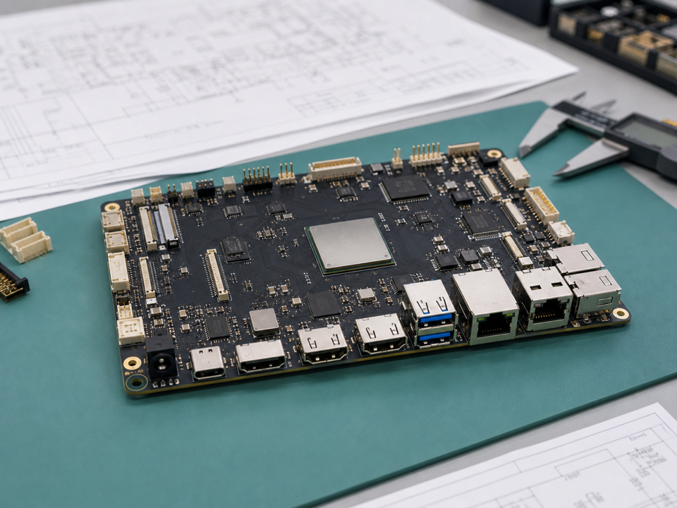
Custom SBC design is not only schematic and PCB layout. It connects mechanical design, component selection, operating system support, BSP work, factory testing, and supply planning. If those topics are handled separately, the first prototype may boot but still fail as a production product.
Start from the enclosure and installation
Mechanical requirements should be collected before schematic and layout decisions become fixed. Product teams should prepare enclosure drawings, board outline limits, mounting holes, connector locations, cable direction, component height limits, keep-out areas, display opening, antenna position, and service access. These details strongly affect placement, routing, test points, and assembly flow.
If the product already has industrial design or a mold, the custom board discussion needs to happen together with mechanical planning. This is especially important for smart terminals, HMI products, gateways, control panels, and wall-mounted devices. A connector that faces the wrong direction can create more trouble than a small electrical issue because it may affect cables, housing, assembly labor, and field service.
For products with displays, the display and touch stack needs review early. Cable length, connector position, backlight power, cover glass, grounding, and touch controller choice can affect both user experience and BSP work. A display that works on a development board may not behave the same way inside the final enclosure.
Define hardware requirements with functions
An interface list should explain what each interface does. “Two USB ports” is less useful than “one USB host for scanner, one internal USB for LTE module.” “UART” should say whether it is debug, RS485, RS232, TTL module communication, or factory use. This level of detail helps the hardware team choose connectors, protection, level shifting, isolation, and test points correctly.
| Requirement area | What to define before layout |
|---|---|
| Display and touch | Interface, resolution, backlight, controller, cable direction |
| Network | Ethernet, Wi-Fi, Bluetooth, LTE, antenna location |
| Control | GPIO, relays, RS485, CAN, inputs, isolation |
| Power | Input voltage, surge, battery, standby, power recovery |
| Mechanics | Outline, holes, height, connectors, service access |
| Production | Flashing, labels, test fixture, serial number, packaging |
The board should be designed for the final assembly process, not only electrical function. Test points need to be reachable. Connectors should be accessible. Antennas should not be buried behind metal. Heat sources should not sit where the enclosure traps heat. These details are easy to discuss early and expensive to fix late.
Choose platform and BSP direction together
Platform choice affects software, cost, and layout. Some products fit Rockchip SBC directions because they need richer Android UI, camera, multimedia, or more processing headroom. Others fit Allwinner SBC directions because cost, compact design, Linux control, audio, or focused I/O matter more. If the product is display and app driven, review Android SBC requirements. If it is a gateway, controller, or unattended device, review Linux SBC requirements.
Do not separate the SoC decision from BSP support. A custom board may change display panel, touch controller, Ethernet PHY, Wi-Fi module, audio codec, PMIC, storage, or camera sensor. Each change can affect Android or Linux adaptation. The official IPC standards resources are useful manufacturing background, but custom SBC success depends on project-specific electrical, mechanical, and software validation.
EVT, DVT, and production thinking
The first prototype should not be treated as the final product. EVT should validate power rails, boot, display, touch, key interfaces, storage, wireless, thermal behavior, and basic BSP. DVT should validate the board inside the real enclosure with real cables, real application software, expected power supply, and longer operation. PVT should validate factory assembly, flashing, functional testing, labels, packaging, and issue feedback.
Production planning should start before PVT. Decide how the image is flashed, how MAC addresses or serial numbers are written, how each interface is tested, how failures are recorded, and how firmware versions are controlled. For more detail, read Custom SBC Development Process and PCBA Production Testing for Embedded SBC Projects.
What buyers should prepare
A good inquiry package needs to cover product photos or drawings, enclosure files, target screen, interface list, operating system, application workflow, power input, expected quantity, sample schedule, certification needs, and any component restrictions. If the product replaces an older device, include what must improve: cost, size, performance, reliability, supply, or installation.
Procurement should also ask about NRE, MOQ, tooling, sample lead time, pilot run plan, BOM control, component alternatives, and lifecycle support. A custom SBC is a product platform, not a one-time PCB job. The best supplier discussion is the one that covers design, BSP, testing, and repeat production from the beginning.
Change control after prototypes
Once EVT samples are built, every change should be treated as a project decision. Moving a connector can affect PCB routing, enclosure parts, cable drawings, test fixtures, and packaging. Changing a wireless module may affect antenna tuning, certification, Linux or Android drivers, and factory test scripts. Changing storage may affect flashing time and image validation.
This does not mean changes should be avoided. EVT exists to find problems. It means each change should have a reason, owner, and validation plan. Keep a simple issue list with hardware revision, image version, test result, proposed fix, and closure status. This record becomes very useful when the project moves from engineering samples to pilot production.
Buyers should also separate must-have changes from nice-to-have improvements. A connector conflict or unstable power rail must be fixed. A minor layout preference may be better held for the next revision if it risks schedule or certification.
Acceptance before production
Before release, prepare a checklist that both customer and supplier can approve. It needs to cover tested interfaces, display and touch status, OS image version, app version, approved BOM, known limitations, test fixture status, packaging requirement, and pilot run result. This keeps production approval from depending on memory or informal messages.
In supplier calls, it helps to open the board drawing and enclosure drawing at the same time. Check screw bosses, cable exit, antenna area, display connector, and test pads together. Five minutes of this review can catch problems that would otherwise wait until the first assembled sample.
Common mistakes to avoid
The first mistake is starting PCB layout before the product shape is stable. If the enclosure, display, or connector plan changes later, the board may need expensive rework. The second mistake is treating BSP as separate from hardware. A new touch controller, wireless module, or Ethernet PHY can change software work. The third mistake is asking for the lowest BOM too early, before the team knows which parts are actually required for reliability and production testing.
For most projects, the better sequence is standard board proof, requirement freeze, custom schematic, EVT validation, DVT in the enclosure, and then pilot production.
Final recommendation
Move to a custom SBC when the product’s enclosure, interfaces, power, display, cost, or production process cannot be handled cleanly by a standard board. Start from mechanical and product requirements, choose the platform with BSP support in mind, validate through EVT/DVT/PVT, and release only when hardware, software, enclosure, and factory test flow are all proven.
Frequently Asked Questions
What details are useful before we talk about a Custom SBC build?
Send the use case, OS preference, display or I/O list, enclosure limits, power input, wireless needs, target quantity, and timing. With that context, Avontek can suggest a Custom SBC hardware path that fits the real device instead of only comparing board specifications.
When is a custom SBC worth considering for a Custom SBC product?
A custom SBC is worth reviewing when the device needs a fixed PCBA outline, connector position, display interface, power input, wireless module, mounting method, or cost target that a catalog board cannot meet cleanly.
Can Avontek stay involved after Custom SBC samples are built?
Yes. Avontek can help with Custom SBC board choice, Android or Linux BSP discussion, peripheral checks, sample bring-up, test fixtures, image review, and factory coordination.